Inhaltsverzeichnis
Product and brand names
All product and brand names used on this website are the property of their respective owners. They are used for identification purposes only.
Even if I mention certain programs or products here, I am not supported by their manufacturer or seller in any way! All posts on my website are private posts without advertising.
The use of my images, text (including excerpts) or other files on your own pages is not permitted without my consent.
Warning
I make this site available to people who are interested in and enjoy electronics and electrical engineering.
Devices in this category (power supplies) contain voltages that are life-threatening. Incorrect handling can therefore endanger your equipment and/or your life!
This description is therefore in no way intended to encourage you to carry out such activities on your own without the necessary specialist knowledge!
Manuals
At the time of the repair, only a user manual in a few versions (e.g. v1.1 dated 18 June 2013 or v2.0 dated 7 January 2015) was available on the internet. However, unlike a service manual, it did not contain any information that could be used during the repair.
Error description
The owner stated that the last time he tried to operate the device, a loud sparking noise was heard and later, after the device was turned over, some small black particles fell out of the device’s casing.
Error verification
The device could be powered on and the LCD and user interface worked, but the output could not be activated. This behavior indicated a problem with one of the device’s secondary circuits.
Build quality
Although the owner emphasized that the unit was purchased new and never repaired, some important components such as rectifiers and power MOSFETs were very sloppily soldered and their solder joints were not cleaned of flux.
In addition, some power components such as rectifier bridges were not completely covered with thermal paste.
Visual inspection
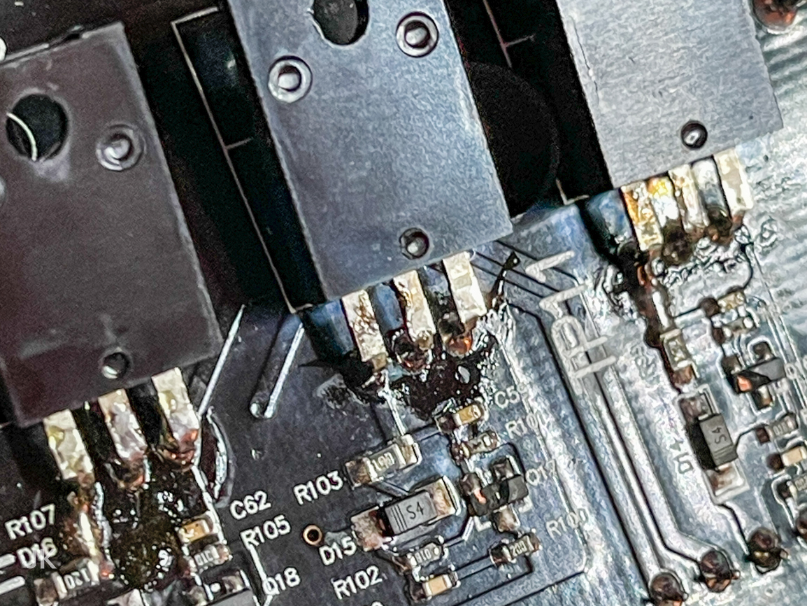
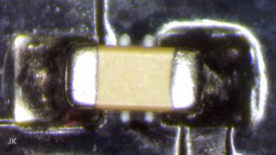
As usual, the check began with a visual inspection of all parts on both sides of the circuit board. The first defects were actually found very quickly – two parts in the SOT-23 package were mechanically damaged.
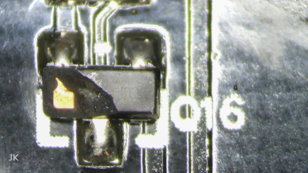
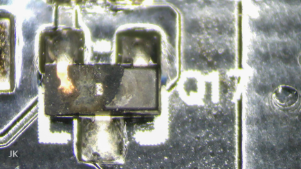
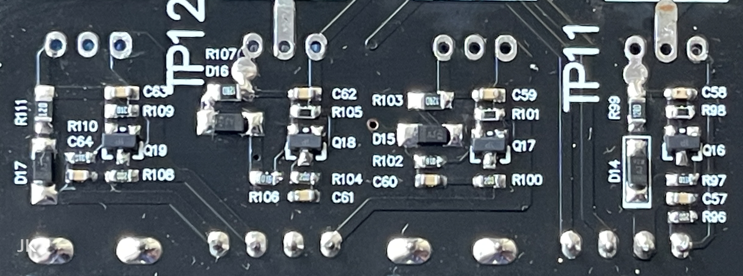
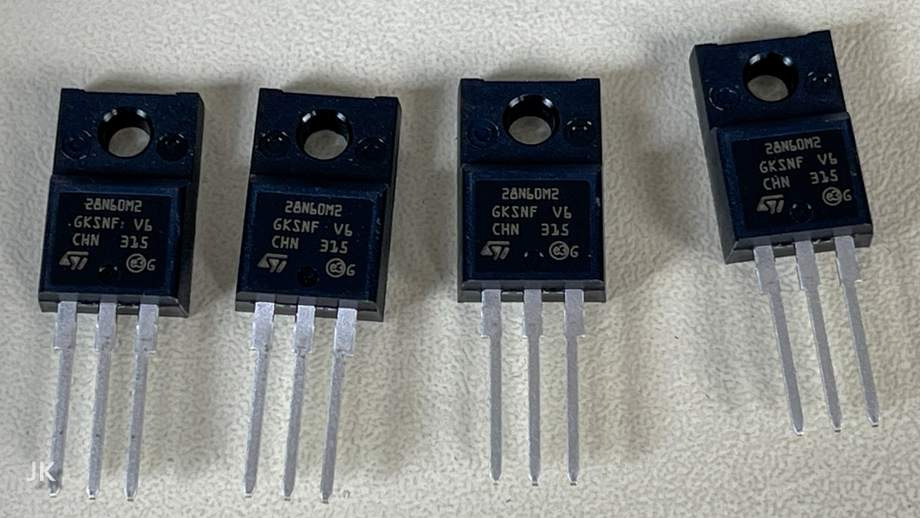
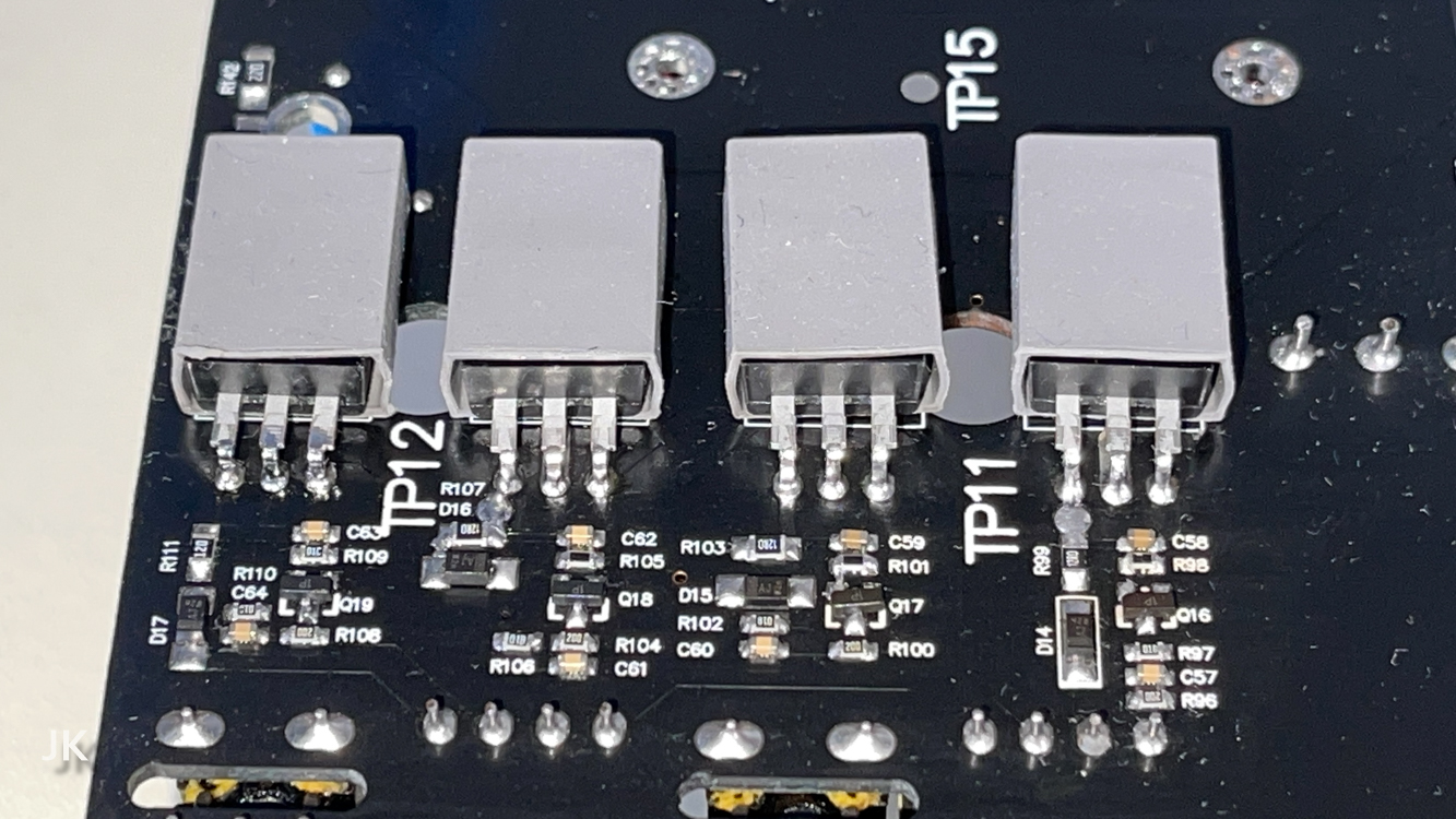
Q16 is part of the external circuit of power MOSFET Q20 and Q17 is part of the external circuit of power MOSFET Q21 (Q20 and Q21 are both 28N60M2 in TO220F package). In addition, some passive components in both circuits were damaged. While some damage was visible to the naked eye, others could only be detected by measurement.
The following pictures show 4 examples.
Problem #1
The mechanically damaged components belong to the circuit that controls the primary side of the main transformer.
Assumptions
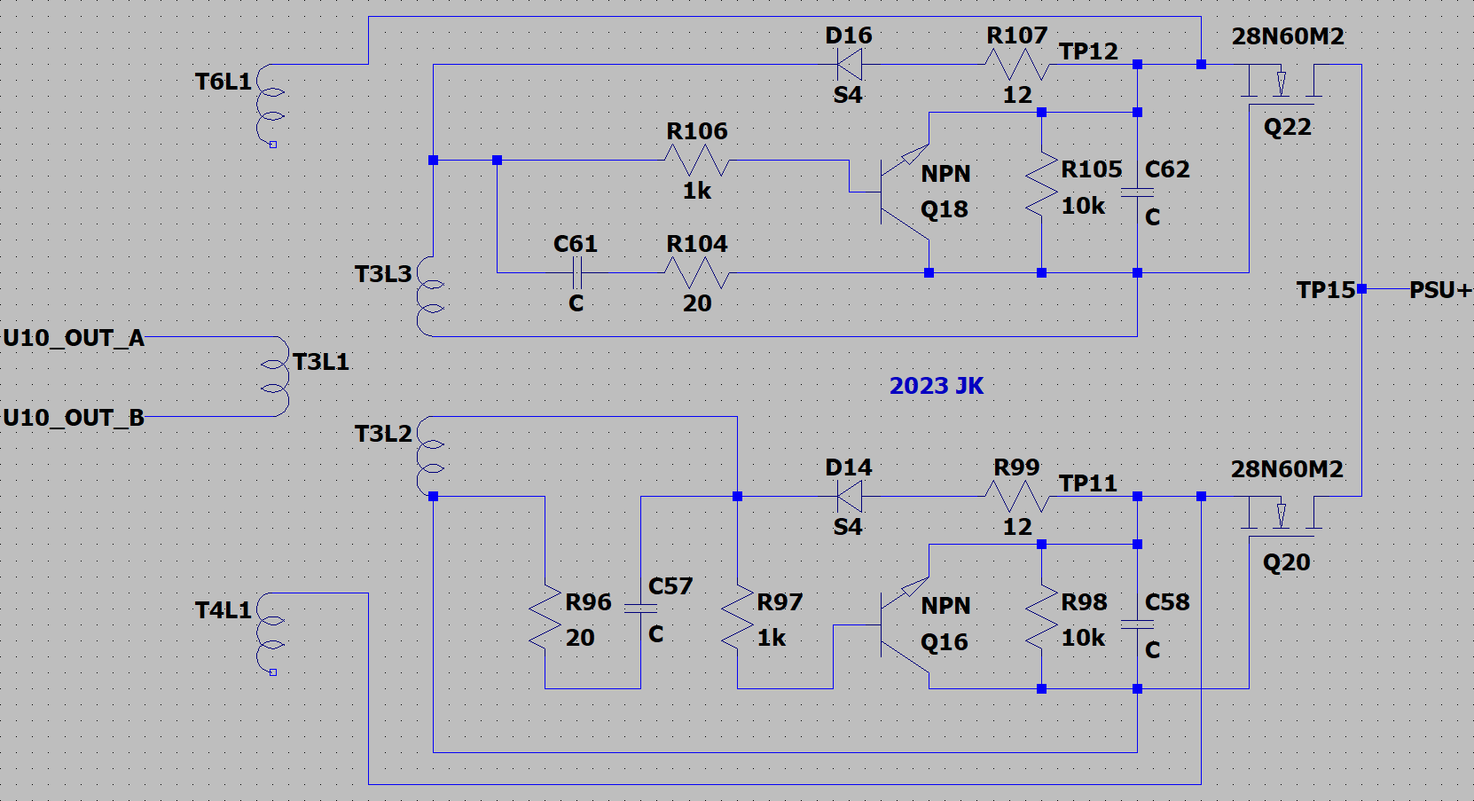
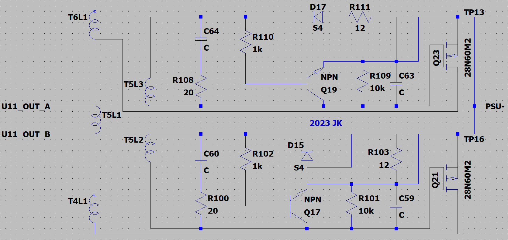
The circuits for Q20, Q21, Q22 and Q23 are similar.
For damaged parts that can no longer be identified, the same type as in the neighboring, comparable circuits is assumed:
Q16=Q18 (MMBT2222A)
Q17=Q19 (MMBT2222A)
Measurements
A dying MOSFET often destroys some other components as well and in fact some random readings on parts near the dead MOSFETs were suspect. More precise measurements gave the results described in the following sections.
All resistor measurements were done using HP/Agilent 34401A 6,5 Digits bench multimeter.
Sentences such as “No component detected!” or “Part is shown as Zener diode!” in the following tables refer to the output of “Peak Atlas DCA75 Pro”.
SMDs near Q20
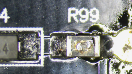
Resistors
| PCB number | Package | Code | Expected value (Ω) | Measured value (Ω) | Replacement value (Ω) |
|---|---|---|---|---|---|
| R69 | 0603 | 200 | 20 | 19.658 * | – |
| R97 | 0603 | 01B | 1 K | 1.0009 K * | – |
| R98 | 0603 | 01C | 10 K | 21.409 K | 10.025 K |
| R99 | 0805 | 120 | 12 | 15 M | 12.151 |
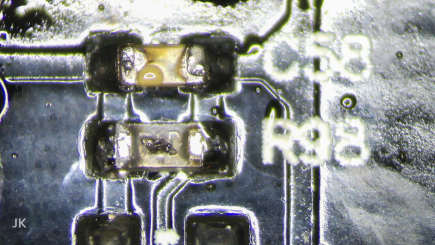
Capacitors
| PCB number | Package | Code | Expected value | Measurement result |
|---|---|---|---|---|
| C57 | 0603 | – | – | Not shorted, but mechanically damaged. * |
| C58 | 0603 | – | – | Not shorted. * |
Although capacitor C58 was electrically unremarkable, its terminals were partially evaporated, which also made it a candidate for replacement.
(Capacity and Dissipation factor @ 1kHz).
Semiconductors
| PCB number | Package | Code | Type | Measurement result | Replacement |
|---|---|---|---|---|---|
| D14 | SOD323 | S4 | 1PS76SB40 | No connection in both directions! * | BAS40H,115 |
| Q16 | SOT-23 | Unreadable | ? | No component detected! Mechanically damaged package! | MMBT2222A |
| Q20 | TO220F | 28N60M2 | 28N60M2 | No component detected! | 28N60M2 |
SMDs near Q21
Resistors
| PCB number | Package | Code | Expected value (Ω) | Measured value (Ω) | Replacement value (Ω) |
|---|---|---|---|---|---|
| R100 | 0603 | 200 | 20 | 19.658 * | – |
| R101 | 0603 | 01C | 10 K | 22.476 K * | 10.030 K |
| R102 | 0603 | 01B | 1 K | 0.99879 K * | – |
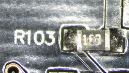
| R103 | 0805 | 120 | 12 | 1.4949 M | 12.174 |
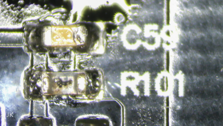
Capacitors
| PCB number | Package | Code | Expected value | Measurement result |
|---|---|---|---|---|
| C59 | 0603 | – | – | Not shorted, but mechanically damaged. * |
| C60 | 0603 | – | – | Not shorted. * |
Semiconductors
| PCB number | Package | Code | Type | Measurement result | Replacement |
|---|---|---|---|---|---|
| D15 | SOD323 | S4 | 1PS76SB40 | No connection in both directions! * | BAS40H,115 |
| Q17 | SOT-23 | Unreadable | ? | No component detected! Mechanically damaged package! | MMBT2222A |
| Q21 | TO220F | 28N60M2 | 28N60M2 | No component detected! | 28N60M2 |
SMDs near Q22
Resistors
| PCB number | Package | Code | Expected value (Ω) | Measured value (Ω) | Replacement value (Ω) |
|---|---|---|---|---|---|
| R104 | 0603 | 200 | 20 | 19.692 * | – |
| R105 | 0603 | 01C | 10 K | 45.261 * 10.006 K | – |
| R106 | 0603 | 01B | 1 K | 360.16 * 0.99769 K | – |
| R107 | 0805 | 120 | 12 | 1.8309 K | 12.195 |
Capacitors
| PCB number | Package | Code | Expected value | Measurement result |
|---|---|---|---|---|
| C61 | 0603 | – | – | Not shorted. * |
| C62 | 0603 | – | – | Not shorted. * |
Semiconductors
| PCB number | Package | Code | Type | Measurement result | Replacement |
|---|---|---|---|---|---|
| D16 | SOD323 | S4 | 1PS76SB40 | Conducting in both directions @ 0.008V. | BAS40H,115 |
| Q18 | SOT-23 | 1P | MMBT2222A ? | Part is shown as Zener diode! | MMBT2222A |
| Q22 | TO220F | 28N60M2 | 28N60M2 | OK | 28N60M2 |
SMDs near Q23
Resistors
| PCB number | Package | Code | Expected value (Ω) | Measured value (Ω) | Replacement value (Ω) |
|---|---|---|---|---|---|
| R108 | 0603 | 200 | 20 | 19.646 * | – |
| R109 | 0603 | 01C | 10 K | 10.035 K * | – |
| R110 | 0603 | 01B | 1 K | 0.99 K * | – |
| R111 | 0805 | 120 | 12 | 11.946 * | – |
Capacitors
| PCB number | Package | Code | Expected value | Measurement result |
|---|---|---|---|---|
| C63 | 0603 | – | – | Not shorted. * |
| C64 | 0603 | – | – | Not shorted. * |
Semiconductors
| PCB number | Package | Code | Type | Measurement result | Replacement |
|---|---|---|---|---|---|
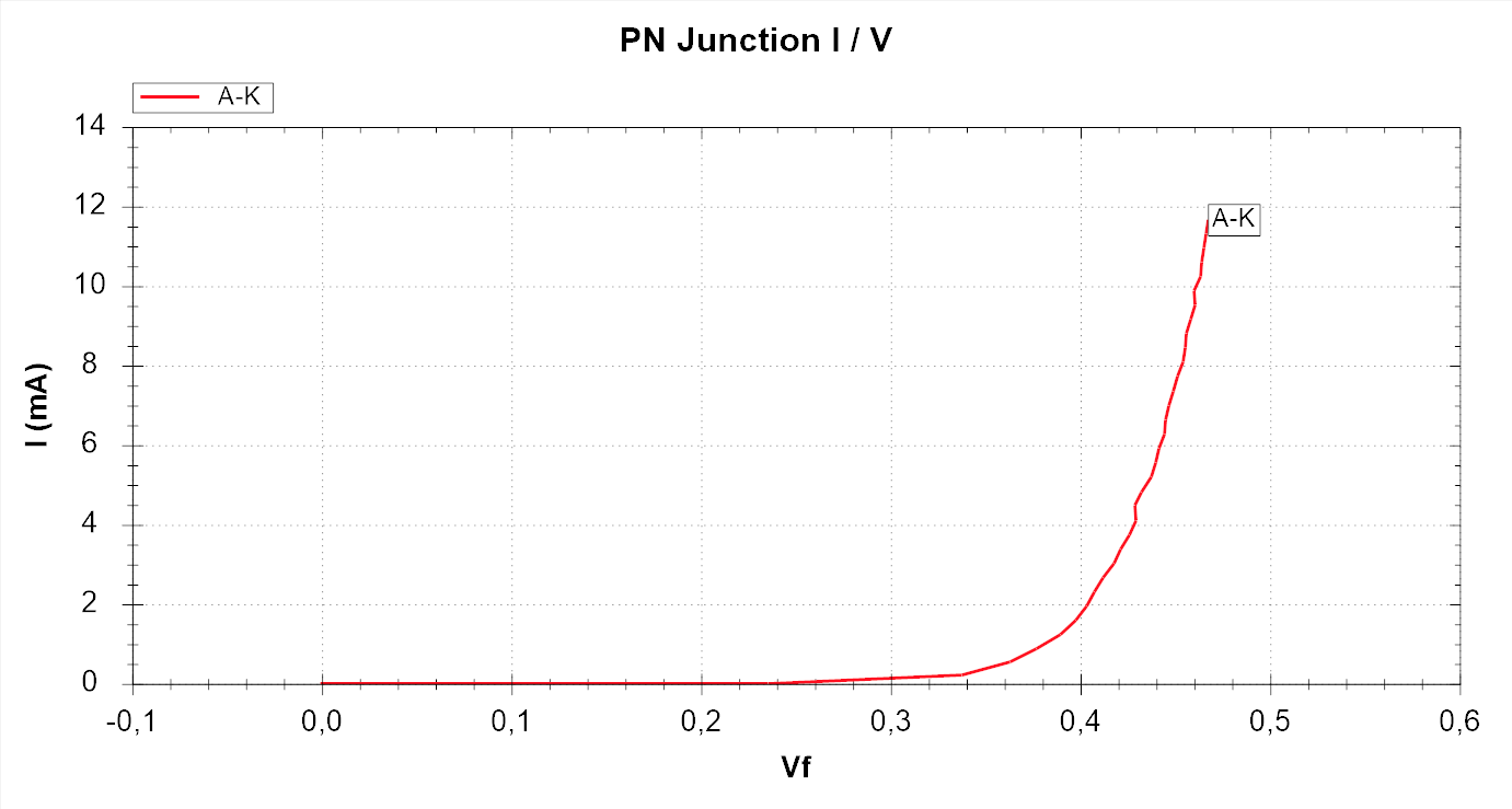
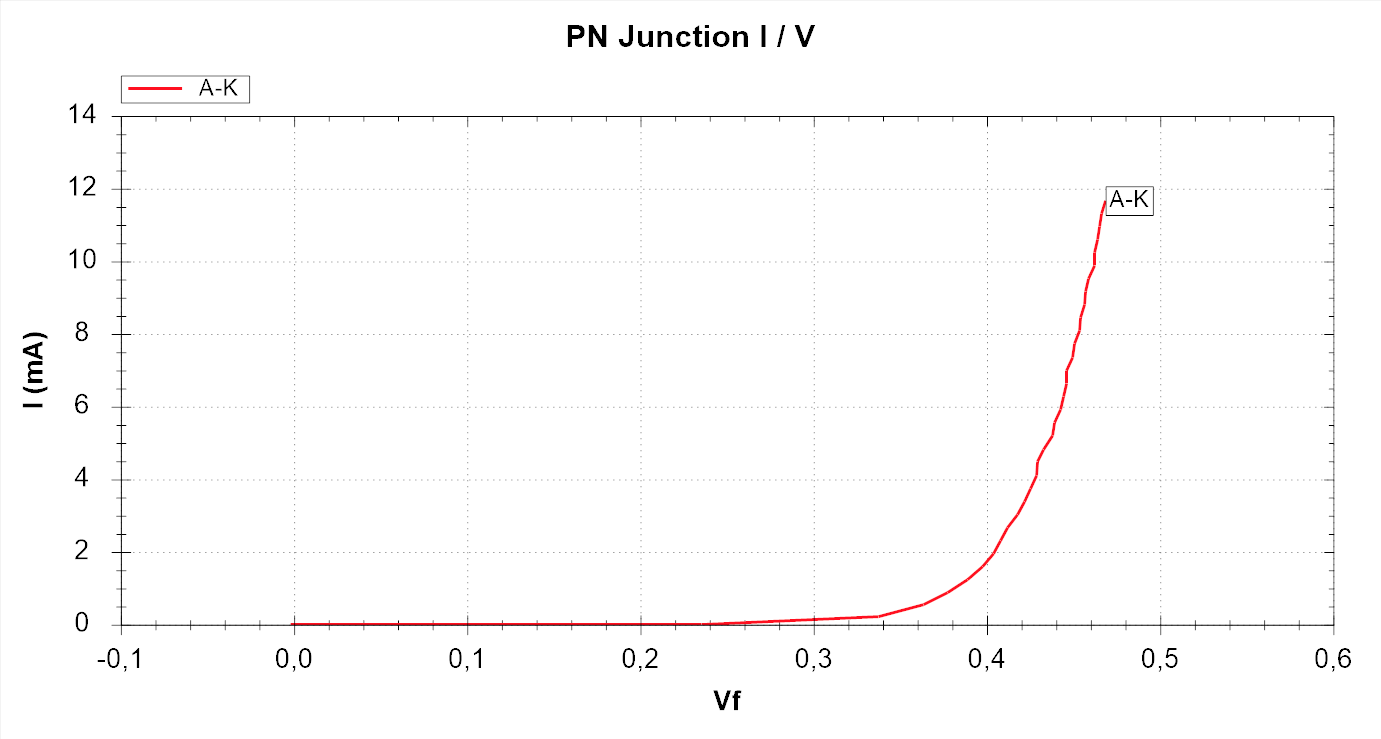
| D17 | SOD323 | S4 | 1PS76SB40 | OK, Vf=0.244V | BAS40H,115 |
| Q19 | SOT-23 | 1P | MMBT2222A ? | Part is shown as Zener diode! | MMBT2222A |
| Q23 | TO220F | 28N60M2 | 28N60M2 | OK | 28N60M2 |
MOSFET Gate Driver
U10 and U11 are TC4424AV (dual 3A MOSFET Gate Driver in SO8 package). U10 controls Q20 and Q22 while U11 controls Q21 and Q23.
Partial circuits
Warning! I do not have a service manual for this device. The circuits in this section are the result of reverse engineering and may be incomplete or even incorrect!
Q20 and Q22
Q21 and Q23
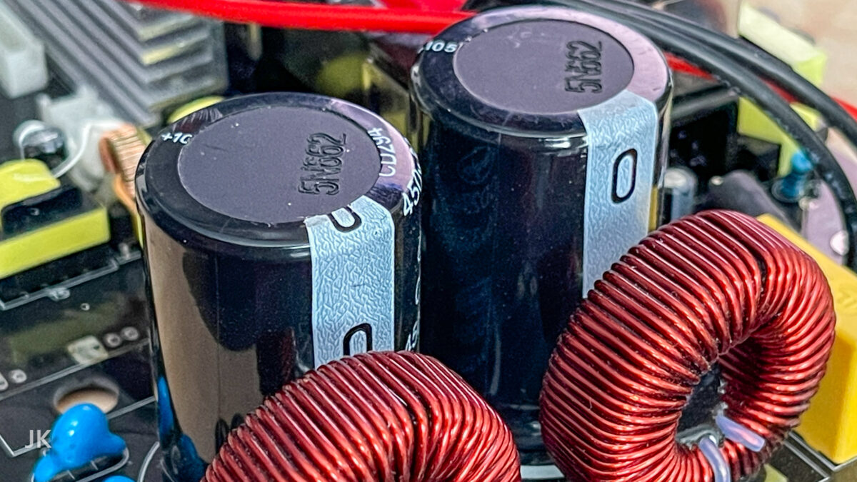
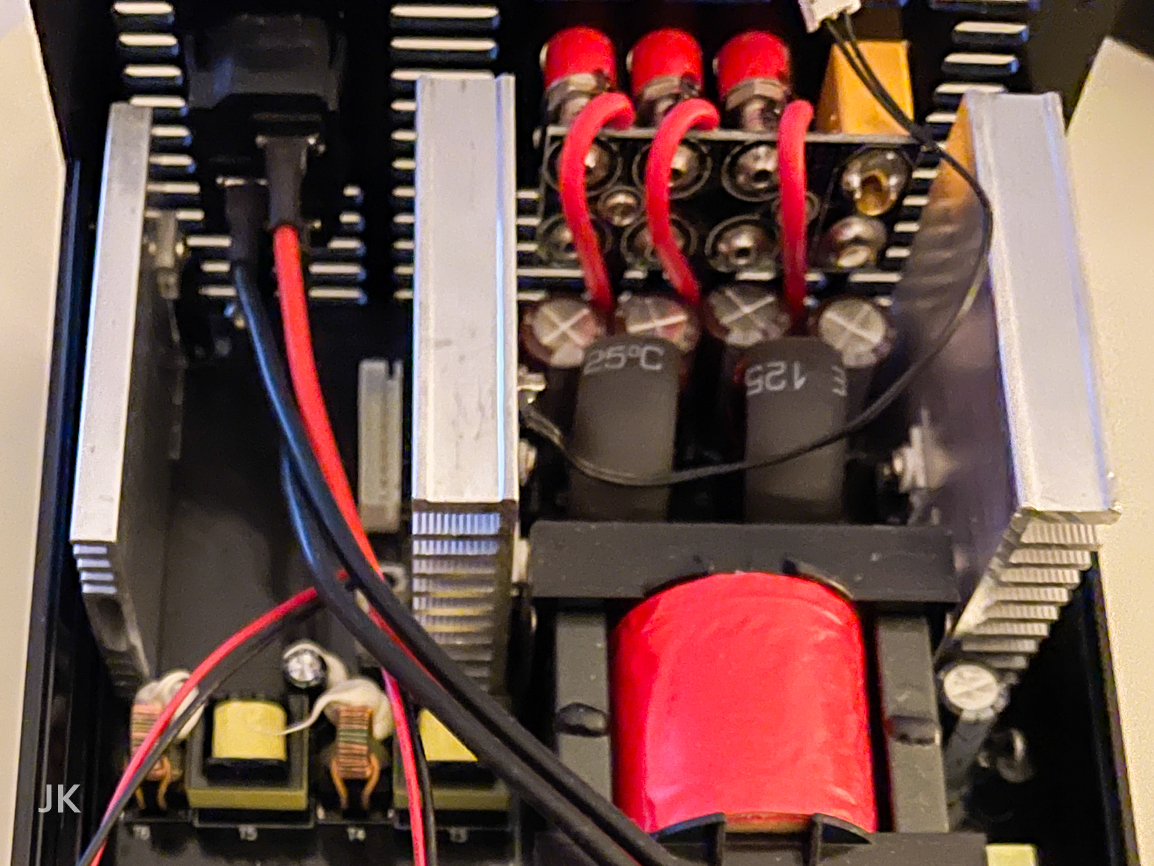
Electrolytic Capacitor Check
Not all capacitor measurements were necessary for this repair, but since the device was already opened I performed these measurements as well.
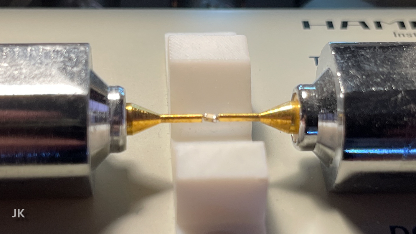
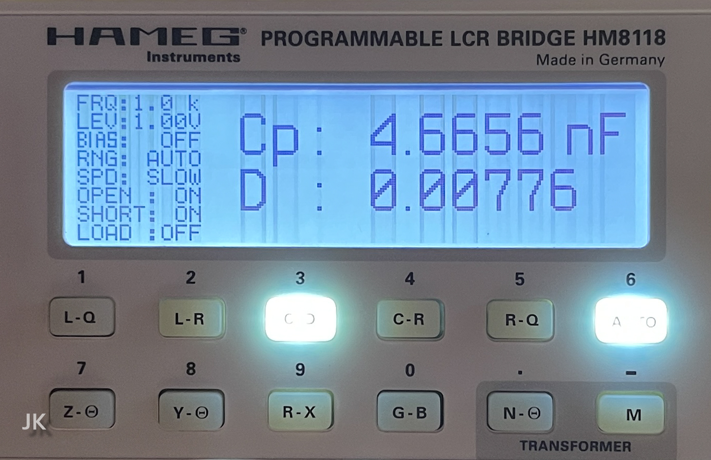
The measurements were performed as In-Circuit measurements using Peak Atlas ESR PLUS ESR70 (Equivalent Series Resistance Meter). E8 and E9 were also additionally measured outside the circuit.
| Part | Parallel connection | Manufacturer & model | Value | Measured value |
|---|---|---|---|---|
| E1 | E1||E2||E3||E4 | CapXon P1610 | 1000µF/35V/+105°C | ?µF, ESR=0.04Ω *2 |
| E2 | E1||E2||E3||E4 | CapXon P1610 | 1000µF/35V/+105°C | ?µF, ESR=0.04Ω *2 |
| E3 | E1||E2||E3||E4 | CapXon P1610 | 1000µF/35V/+105°C | ?µF, ESR=0.03Ω *2 |
| E4 | E1||E2||E3||E4 | CapXon P1610 | 1000µF/35V/+105°C | ?µF, ESR=0.04Ω *2 |
| E5 | – | CapXon ? | 1000µF/25V/+105°C | 1086µF, ESR=0.04Ω |
| E6 | – | CapXon ? | 100µF/25V/+105°C | ?µF, ESR=0.08Ω *2 |
| E7 | – | CapXon P1604 | 100µF/35V/+105°C | 113.0µF, ESR=0.24Ω |
| E8 | E8||E9 | Jianghai CD294 | 330µF/450V/+105°C | 602.6µF, ESR=0.10Ω *1 304.3µF 0.12Ω |
| E9 | E8||E9 | Jianghai CD294 | 330µF/450V/+105°C | 603.6µF, ESR=0.08Ω *1 298.8µF 0.14Ω |
*2 In-Circuit measurement, but the result was not available, not plausible or only partially available.
Not all measurements in the circuit produced a useful result, but at least they did not indicate a problem. So there was no need to desolder in this case.
Additional measurements
| Part number | Package | Type | Result |
|---|---|---|---|
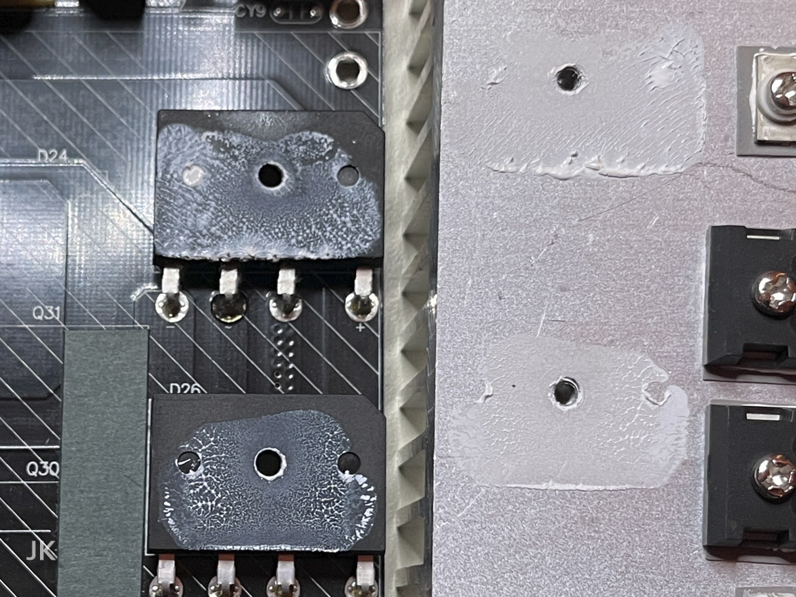
| D24 | TO220 | 1F32AV | OK Vf=0.435V @ 5.00mA IV Chart |
| D25 | TO220 | 1F32AV | OK Vf=0.435V @ 5.00mA IV Chart |
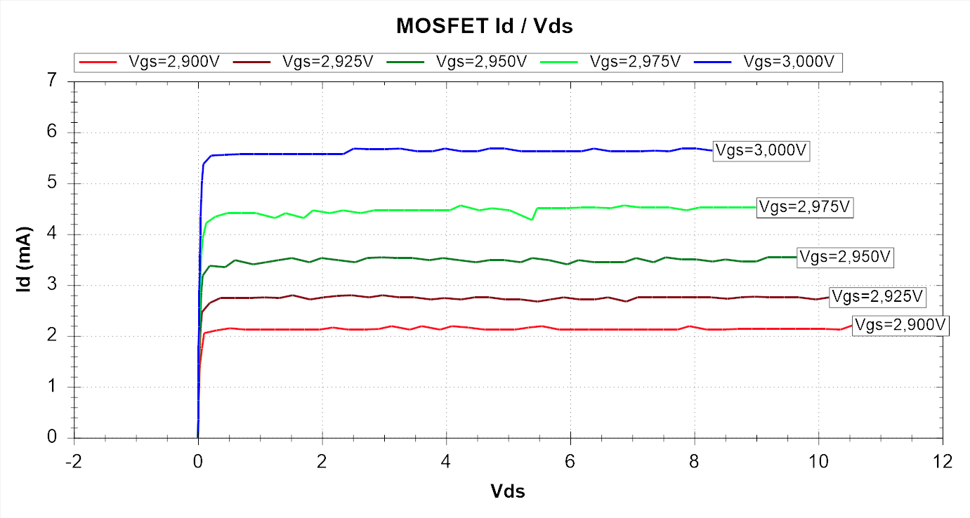
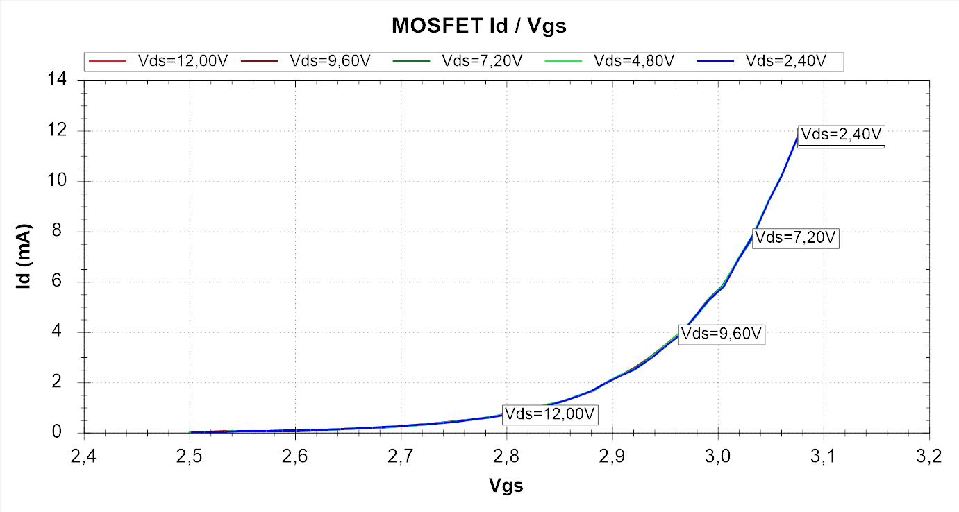
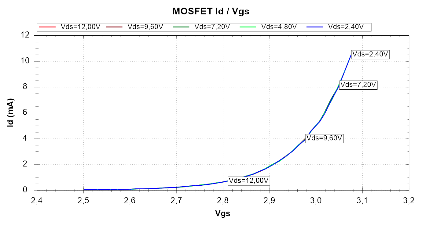
| Q30 | TO247 | 47N60C3 | OK, further data in the table below. |
| Q31 | TO247 | 47N60C3 | OK, further data in the table below. |
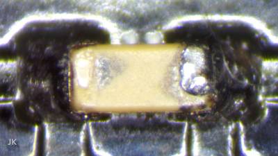
| C58 | 0603 | 4.7 nF | Mechanically damaged! |
| C59 | 0603 | 4.7 nF | Mechanically damaged! |
| Q30 | Q31 | |
|---|---|---|
| Type | N-Ch Enhancement mode MOSFET with body diode | N-Ch Enhancement mode MOSFET with body diode |
| Vgs(on) | 2.985V at Id=5.02mA and Ig=3µA | 2.998V at Id=5.03mA and Ig=1µA |
| Vgs(off) | 2.305V at Id=4.9µA | 2.327V at Id=5.2µA |
| gm | 40.8mA/V at Id=3.0mA to 5.0mA | 38.8mA/V at Id=3.0mA to 5.0mA |
| Rds(on) | <1.0Ω at Id=5.0mA and Vgs=8.0V | <1.0Ω at Id=5.0mA and Vgs=8.0V |
| Charts | Id/Vds, Id/Vgs | Id/Vds, Id/Vgs |
Replacements
Replaced parts #1
| Part | Package | Part numbers |
|---|---|---|
| 28N60M2 | TO220F | Q20, Q21, Q22, Q23 |
| MMBT2222A (1P) | SOT-23 (SMD) | Q16, Q17, Q18, Q19 |
| 1PS76SB40 (S4) | SOD323 (SMD) | D14, D15, D16, D17 |
| 10k | 0603 (SMD) | R98, R101 |
| 12Ω | 0805 (SMD) | R99, R103, R107 |
| 4,7 nF | 0603 (SMD) | C58, C59 |
Q22 and Q23 passed the test, but I usually replace all power MOSFETs of an affected H-bridge.
Problem #2
During the measurements I have noticed that the output resistance of the PSU is very low (less than 1 ohm). So there was also an error on the secondary side.
The search for the defective component using a thermal imaging camera led to nothing. Even after injecting 8.5 A, no component became significantly warmer and the leads were shown as the warmest components. I assumed that the defective component was on a cooling plate and was therefore not easy to find using this method.
Since there was no free access to the MOSFET screws, the MOSFETs and heat sinks had to be desoldered together for further tests. To protect the circuit board, the original solder was first vacuumed out, replaced with a solder with a low melting temperature and then vacuumed out again.
The short circuit disappeared after removing the third (middle) heatsink, which carries the power MOSFETS Q3 and Q4 as well as the temperature sensor.
The out-of-circuit power MOSFET measurements confirmed the malfunction of Q3. This was also consistent with the images previously taken with the thermal imaging camera, which were not meaningful on their own. During the IR study, coil L2, which has direct connection to Q3 and Q4, was slightly warmer (1 to 2°C) than coil L1.
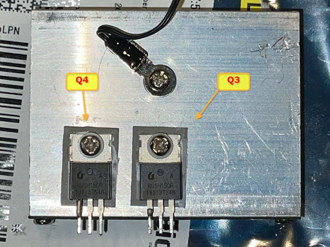
| Part number | Package | Component type | Model | Check results |
|---|---|---|---|---|
| Q1 | TO220 | N-Channel Advanced Power MOSFET | RU1H150R | OK |
| Q2 | TO220 | N-Channel Advanced Power MOSFET | RU1H150R | OK |
| Q3 | TO220 | N-Channel Advanced Power MOSFET | RU1H150R | Failed! All 3 leads shorted. |
| Q4 | TO220 | N-Channel Advanced Power MOSFET | RU1H150R | OK |
| Q5 | TO220 | Bipolar Junction Transistor (BJT) | 1508 J13009-2 | OK |
Replacement Q3, Part #1
The RU1H150R is a Chinese semiconductor, but it was not easy to find.
To avoid getting a fake, I wanted to buy the part from companies that specialize in it. Although the component was listed in the webshop in some cases, my request was rejected with the note that it was currently not available.
After a long, unsuccessful search, I finally tried one of the sites where almost everything is sold. The item description indicated that it was guaranteed to be an original.
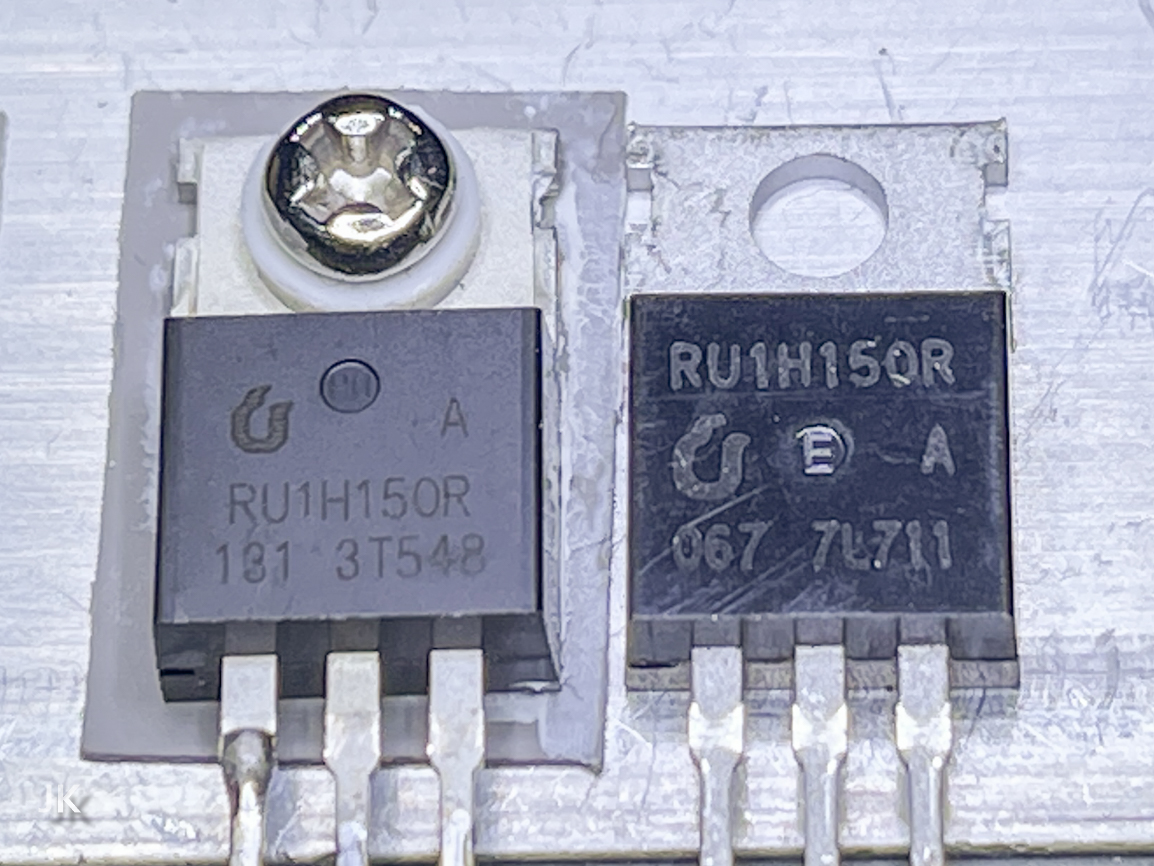
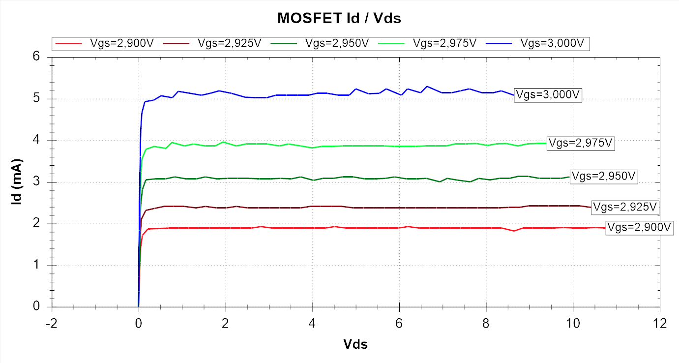
| Original Q3 | Replacement part #1 | |
|---|---|---|
| Type | N-Ch Enhancement mode MOSFET with body diode | N-Ch Enhancement mode MOSFET with body diode |
| Vgs(on) | 3.478V at Id=5.01mA and Ig=0µA | 3.581V at Id=5.01mA and Ig=0µA |
| Vgs(off) | 2.279V at Id=5.1µA | 2.781V at Id=5.1µA |
| gm | 34.0mA/V at Id=3.0mA to 5.0mA | 37.2mA/V at Id=3.0mA to 5.0mA |
| Rds(on) | <1.0Ω at Id=5.0mA and Vgs=8.0V | <1.0Ω at Id=5.0mA and Vgs=8.0V |
In my opinion, the results of these spare parts deviated too much from the original and I therefore decided to replace them with parts from a known good source.
Replacement Q3, Part #2
As described in previous section I have decided to go for another part from a trustworthy source.
After comparing the parameters of many available components from well-known electronics suppliers, I am convinced that I have finally found a component that will do its job perfectly for years to come:
CSD19536KCS N-CH MOSFET 100V 150A TO220-3
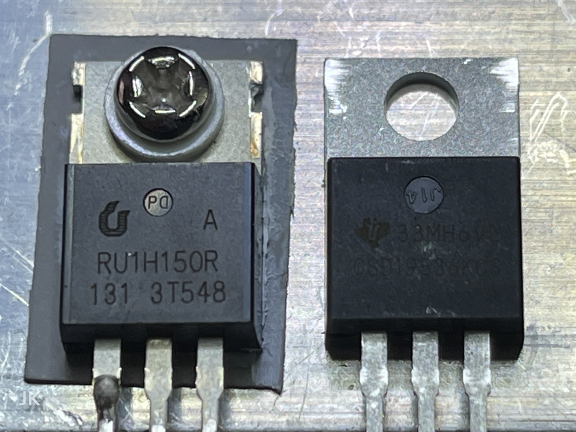
| Original Q3 | Replacement part #2 | |
|---|---|---|
| Type | N-Ch Enhancement mode MOSFET with body diode | N-Ch Enhancement mode MOSFET with 0,57Vf body diode |
| Vgs(on) | 3.478V at Id=5.01mA and Ig=0µA | 2.843V at Id=5.00mA and Ig=0µA |
| Vgs(off) | 2.279V at Id=5.1µA | 2.059V at Id=5.1µA |
| gm | 34.0mA/V at Id=3.0mA to 5.0mA | 341.3mA/V at Id=3.0mA to 5.0mA |
| Rds(on) | <1.0Ω at Id=5.0mA and Vgs=8.0V | <1.0Ω at Id=5.0mA and Vgs=8.0V |
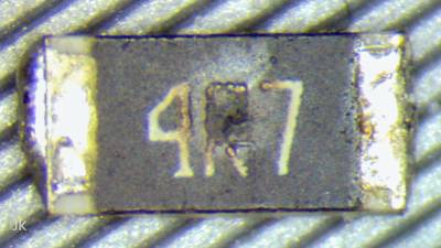
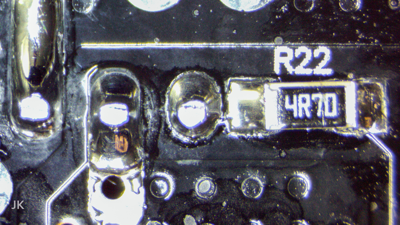
R22
R22 is the gate resistor of Q3 and it was also destroyed. The selected replacement part is Yageo RC1206FR-134R7 (4R7/0,25W/1%/200V/100ppm).
| PCB number | Package | Code | Expected value (Ω) | Measured value (Ω) | Replacement value (Ω) |
|---|---|---|---|---|---|
| R22 | 1206 | 4R7 | 4R7 | 2K9 | 4R696 |
Replaced parts #2
| Part | Package | Part numbers |
|---|---|---|
| CSD19536KCS | TO220-3 | Q1, Q2, Q3, Q4 |
| 4R7 | 1206 (SMD) | R22 |
As mentioned before, I usually replace all power MOSFETs of an affected H-bridge and in this case I also selected a new power MOSFET type. Therefore, the non-defective power MOSFETs Q1, Q2 and Q4 were also replaced.
Verification
Power-On
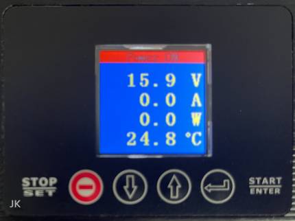
The function was confirmed by measurements at the output at different output voltages.
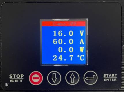
Load Test
The power supply can deliver 1500 W and therefore cannot be fully tested with my “Rigol DL3031A Electronic Load 150 VDC/60 A/350 W” due to its limited power, but this test is at least better than pure idle measurements.
The connection between the D.U.T. (=Device Under Test) and the electronic load was realized using 2 cable sets suitable for 20A each and separate measuring cables.
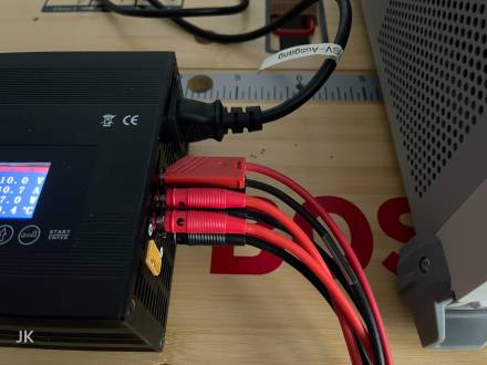
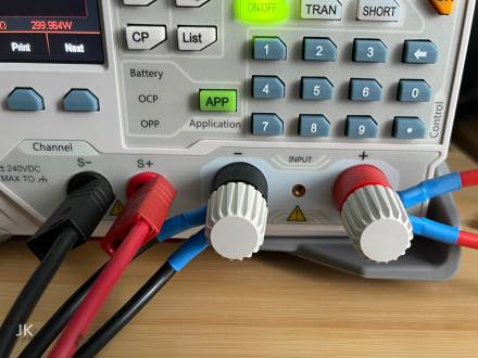
No problems were detected even after a longer period of operation with a load of 300W. After a short time, both fans of the power supply started up, so that no excessive temperature increase could be detected in the test.
Digital obsolescence
The power supply is relatively well built and can be maintained or repaired relatively easily. I would have given the manufacturer almost 10 out of 10 points if he hadn’t taken a step towards digital obsolescence.
It is true that a service manual is almost never available for modern electronics, but in many cases you can live with that.
What I can’t stand, however, is the grinding off of the ICs. There are 3 ICs in this power supply with sanded off labels.